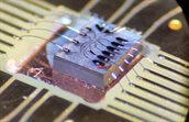
Specialised Diamond Chip Fab
Color centers in diamond chips have widespread applications in a variety of advanced technological fields. But there are currently no foundries that can produce these chips. So, companies and academia must spend valuable time and resources designing, building, and testing the chips themselves before they develop their innovations. TNO’s diamond devices roadmap aims to develop scalable processes to accelerate production of state-of-the-art diamond chips.
Driving innovation
Color centers in diamond can maintain quantum states and interact with extreme sensitivity with their environment. This makes them ideally suited for a multitude of quantum applications, but also for biomedical technology, advanced electronics, and highly sensitive detectors and sensors. More and more companies are positioning themselves to become early developers of diamond-based technologies. However, the time and investment required to develop and test their own chips is delaying development and threatening companies’ competitive advantage.
The European Chips Act is set to advance the EU’s position in the global chips market by developing chip foundries, both for established and next-generation technologies. In addition, thanks to government funding, the Netherlands has become a world leader in the field of diamond-based quantum technology, and is therefore an ideal location for a comprehensive chip fabrication facility (‘fab’). TNO aims to make use of that momentum and become the leading manufacturer of diamond device microchips.
Roadmap for success
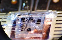
TNO has long-standing and extensive experience in the design, automatic characterisation, and fabrication of diamond chips. Today, the TNO diamond devices roadmap includes the development of scalable, accessible, and efficient fabrication processes. We aim to develop fabrication processes that work for multiple clients at the same time, thereby reducing time and cost for each individual customer.
One potential approach is Multiple Project Wafers (MPWs), and the use of an open interface Process Development Kit (PDK). With this approach, the fabrication process is fixed, but custom device designs from multiple users can be combined in a single fabrication run. This approach allows us to (re-)use existing fabrication expertise, optimise the MPW process, and enable scalability and cost savings across the board.
Reducing time to market
TNO foresees sufficient market for a specialised diamond chip fab. We envision that the commercialisation of this technology, for instance by means of a spin-off, could lead to the development of the world’s most reputable diamond chip fab. By offering our expertise, technology, and facilities to the entire diamond device ecosystem, we aim to provide higher quality chips, faster and easier than is possible through independent development.
Instead of spending vast amounts of time and research funding to develop their own chips, companies can outsource the production to accelerate the development of diamond-based systems and enable a first-to-market advantage over competitors. Academia can focus on their core research and accelerate the developments that will lead to breakthrough discoveries and applications.
Experience that matters
TNO is already offering its proven techniques, expertise, and facilities for small-batch chip production, and our patented and proven recipes can be available in a variety of partnership or licensing agreements. Thus, the full power of this knowledge – and the facilities that support it – are ready to drive innovation and accelerate advancements that will benefit society as a whole. From quantum computing, sensing, and communication to high resolution medical imaging, magnetic field sensing, and industrial sensors.
In the early stages of this Tech Transfer, the potential chip foundry is exploring the ways in which it can have the most profound impact on the industry and the ecosystem. Investors and partners interested in finding out more should get in touch to discuss the possibilities to include this remarkable technology in their Research & Development activities.
Could Specialised Diamond Chip Fab technology benefit your market position? Contact us for investment and/or development opportunities.
Contact
-

Rolph Segers
Functie:Tech Transfer OfficerSpecialisatie niet bekendRolph is involved in bringing technology to the market by setting up spin-off or deep-tech startup companies at TNO. He is also responsible for creating workshops and e-learning modules for deep-tech startups. If you're an early-stage investor or entrepreneur interested in TNO's spin-offs, feel free to get in touch with him.
-
E-mail:E-mail Rolph
-
LinkedIn:Rolph on LinkedIn
-